Comodity DRAM PRODUCTS
Introduction
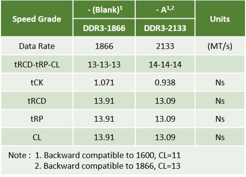
The JSC DDR3 product family operates normal voltage at 1.5V, and low voltage at 1.35V. Both are organized as 8 I/Os x 8banks in 78-ball BGA and 16 I/Os x 8banks in 96-ball BGA .

Features
● Differential bidirectional data strobe● Data masking per byte on Write commands
● Programmable Burst length of 4 or 8
● Programmable CAS (READ) latency (CL)
● Programmable posted CAS additive latency (AL)
● Programmable CAS (WRITE) latency (CWL)
● OCD (Driver Adjustment)
● ODT (On Die Termination) supported
● Write Leveling
● Packages: 96-ball BGA for x16, 78-ball BGA for x8
● Long-term support
| Density | Bus | Voltage | Max Frequancy | Package Type | Part Number | Status |
|---|---|---|---|---|---|---|
| 8Gb | x16 | 1.2V | 1600MHz | 96B (7.5x13.3mm) | LPR4B8G168LAHS-05B | M/P |
| 16Gb | x16 | 1.2V | 1600MHz | 96B (9.5x13.3mm) | LPR4BAG168LAHK-05B | Sample Now |
| Density | Bus | Voltage | Max Frequancy | Package Type | Part Number | Status |
|---|---|---|---|---|---|---|
| 2Gb | x16 | 1.5V | 933MHz | 96B (7.5x13.3mm) | JSR362G168NHR | M/P |
| 2Gb | x16 | 1.5V | 933MHz | 96B (7.5x13mm) | JSR362G168NHR-I | M/P |
| 2Gb | x16 | 1.5V | 1066MHz | 96B (7.5x13mm) | JSR362G168NHR-A | M/P |
| 2Gb | x16 | 1.5V | 1066MHz | 96B (7.5x13mm) | JSR362G168NHR-AI | M/P |
| 2Gb | x8 | 1.5V | 933MHz | 78B (7.5x11.0mm) | JSR362G088NHW | M/P |
| 2Gb | x8 | 1.5V | 933MHz | 78B (7.5x11.0mm) | JSR362G088NHW-I | M/P |
| 2Gb | x8 | 1.5V | 1066MHz | 78B (7.5x11.0mm) | JSR362G088NHW-A | M/P |
| 2Gb | x8 | 1.5V | 1066MHz | 78B (7.5x11.0mm) | JSR362G088NHW-AI | M/P |
| 4Gb | x16 | 1.5V | 933MHz | 96B (7.5x13mm) | JSR364G168NHR | M/P |
| 4Gb | x16 | 1.5V | 933MHz | 96B (7.5x13mm) | JSR364G168NHR-I | M/P |
| 4Gb | x16 | 1.5V | 1066MHz | 96B (7.5x13mm) | JSR364G168NHR-A | M/P |
| 4Gb | x16 | 1.5V | 1066MHz | 96B (7.5x13mm) | JSR364G168NHR-AI | M/P |
| 4Gb | x8 | 1.5V | 933MHz | 78B (7.5x11.0mm) | JSR364G088NHW | M/P |
| 4Gb | x8 | 1.5V | 933MHz | 78B (7.5x11.0mm) | JSR364G088NHW-I | M/P |
| 4Gb | x8 | 1.5V | 1066MHz | 78B (7.5x11.0mm) | JSR364G088NHW-A | M/P |
| 4Gb | x8 | 1.5V | 1066MHz | 78B (7.5x11.0mm) | JSR364G088NHW-AI | M/P |
| Density | Bus | Voltage | Max Frequancy | Package Type | Part Number | Status |
|---|---|---|---|---|---|---|
| 2Gb | x16 | 1.35V | 933MHz | 96B (7.5x13mm) | JSR362G168NHR-L | M/P |
| 2Gb | x16 | 1.35V | 933MHz | 96B (7.5x13mm) | JSR362G168NHR-LI | M/P |
| 2Gb | x16 | 1.35V | 1066MHz | 96B (7.5x13mm) | JSR362G168NHR-LA | M/P |
| 2Gb | x16 | 1.35V | 1066MHz | 96B (7.5x13mm) | JSR362G168NHR-LAI | M/P |
| 2Gb | x8 | 1.35V | 933MHz | 78B (7.5x11.0mm) | JSR362G088NHW-L | M/P |
| 2Gb | x8 | 1.35V | 933MHz | 78B (7.5x11.0mm) | JSR362G088NHW-LI | M/P |
| 2Gb | x8 | 1.35V | 1066MHz | 78B (7.5x11.0mm) | JSR362G088NHW-LA | M/P |
| 2Gb | x8 | 1.35V | 1066MHz | 78B (7.5x11.0mm) | JSR362G088NHW-LAI | M/P |
| 4Gb | x16 | 1.35V | 933MHz | 96B (7.5x13mm) | JSR364G168NHR-LI | M/P |
| 4Gb | x16 | 1.35V | 1066MHz | 96B (7.5x13mm) | JSR364G168NHR-LA | M/P |
| 4Gb | x16 | 1.35V | 1066MHz | 96B (7.5x13mm) | JSR364G168NHR-LAI | M/P |
| 4Gb | x8 | 1.35V | 933MHz | 96B (7.5x13mm) | JSR364G168NHR-L | M/P |
| 4Gb | x8 | 1.35V | 933MHz | 78B (7.5x11.0mm) | JSR364G088NHW-L | M/P |
| 4Gb | x8 | 1.35V | 933MHz | 78B (7.5x11.0mm) | JSR364G088NHW-LI | M/P |
| 4Gb | x8 | 1.35V | 1066MHz | 78B (7.5x11.0mm) | JSR364G088NHW-LA | M/P |
| 4Gb | x8 | 1.35V | 1066MHz | 78B (7.5x11.0mm) | JSR364G088NHW-LAI | M/P |

 Comodity DRAM Product Overview
.png)